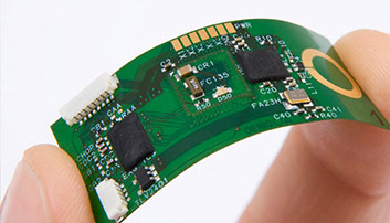
It is useful to remember that most of the traditional board designs are simple digital designs. Routing and placing the bypass capacitors in the designs are very simple. As the designs grow in both speed and complexity, the requirement of designing a refined PDN (power distribution network) on the circuit boards is increased. Now with signal integrity needs of the high-speed design, an accurately designed PDN is imperative for superior performance of a circuit board. If you know requirements of bypass capacitor in the PDN of high-speed design, you can read this article. It not only provides you certain useful details but also let you know about the right kind of routing and placement strategies. The IC’s and processor on any high-speed PCB demand the sharp current spike that a power supply fails to delivery. The power supply is designed for supply the required range of power across an entire board apart from short bursts. For solving this problem, the bypass capacitors are placed close to the IC for supply the desired current for quick spikes.
Why use bypass capacitors?
The bypass capacitors perform this task by storing enough power and discharging it correctly to the IC while it needs additional current. They are also essential to reduce ground bounce which can come from the digital devices which have quick switching times. Apart from that, they are used for filtering lower-frequency noise creating by your power supply. They are also helpful with some other EMI and signal integrity issues. The number of capacitors required for High Speed PCB Design is based on the parts which they are actually assigned to. The bulk capacitors with 10uF range are commonly used for every voltage on the digital board. The capacitors are placed where the required voltage is developed. On some other devices, bypass capacitors are utilized in combination with some high-speed bypass capacitors.
Best practice to route and place bypass capacity
It is essential to place the bypass capacitor near the device which they are actually assigned to. It can be below the device or simply off pins that a bypass capacitor is connected to in a similar direction of a board. If the circuits need many bypass capacitors positioned near a power pin of a particular device, you should place the capacitor next to a pin in the ascending order. For example, if both the 10 uF and .01 uF capacitors are assigned for a particular device, you can place .01 uF near to a device with 10 uF capacitor which is near to a device pin. While you are routing your bypass capacity, you can begin from the ground or power pin of your device and go straight to a capacitor pin. You can also utilize as wide and short traces as possible for connecting your bypass capacity. You can also use several visas for connecting the ground plane or power plane as possible. In short, routing and placement of the bypass capacitors for an effective PDN is an essential portion of High Speed PCB Design. If you want to achieve the best results, you can follow the tips and use the best resources to resolve PDN issues.


